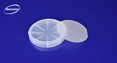
2 inch GaN Template
| Item | GaN-T-C-U-C50 | GaN-T-C-N-C50 | GaN-T-C-P-C50 |
| Dimensions | Ф50.8 ± 0.1 mm | Ф50.8 ± 0.1 mm | Ф50.8 ± 0.1 mm |
| Thickness | 4.5±0.5 µm, 20±2 µm | 4.5±0.5 µm, 20±2 µm | 4.5±0.5 µm |
| Orientation | C-plane(0001) ± 0.5° | C-plane(0001) ± 0.5° | C-plane(0001) ± 0.5° |
| Conduction Type | N-type(Undoped) | N-type(Si-doped) | P-type(Mg-doped) |
| Resistivity(300K) | < 0.5Ω·cm | < 0.05Ω·cm | ~10Ω·cm |
| Carrier Concentration | < 5x1017cm-3 | > 1x1018cm-3 | > 6x1016cm-3 |
| Mobility | ~ 300cm2/V•s | ~ 200cm2/V•s | ~ 10cm2/V•s |
| Dislocation Density | Less than 5x108 cm-2(estimated by FWHMs of XRD) | Less than 5x108 cm-2(estimated by FWHMs of XRD) | Less than 5x108cm-2(estimated by FWHMs of XRD) |
| Substrate Structure | GaN on sapphire (standard :SSP option:DSP) | GaN on sapphire (standard :SSP option:DSP) | GaN on sapphire (standard :SSP option:DSP) |
| Useable Surface Area | >90% | >90% | >90% |
| Package | Packaged in a class 100 clean room environment, in cassette of 25pcs | Packaged in a class 100 clean room environment, in cassette of 25pcs | Packaged in a class 100 clean room environment, in cassette of 25pcs |
| or single container , under a nitrogen atmosphere. | or single container , under a nitrogen atmosphere. | or single container , under a nitrogen atmosphere. |
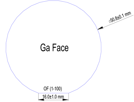
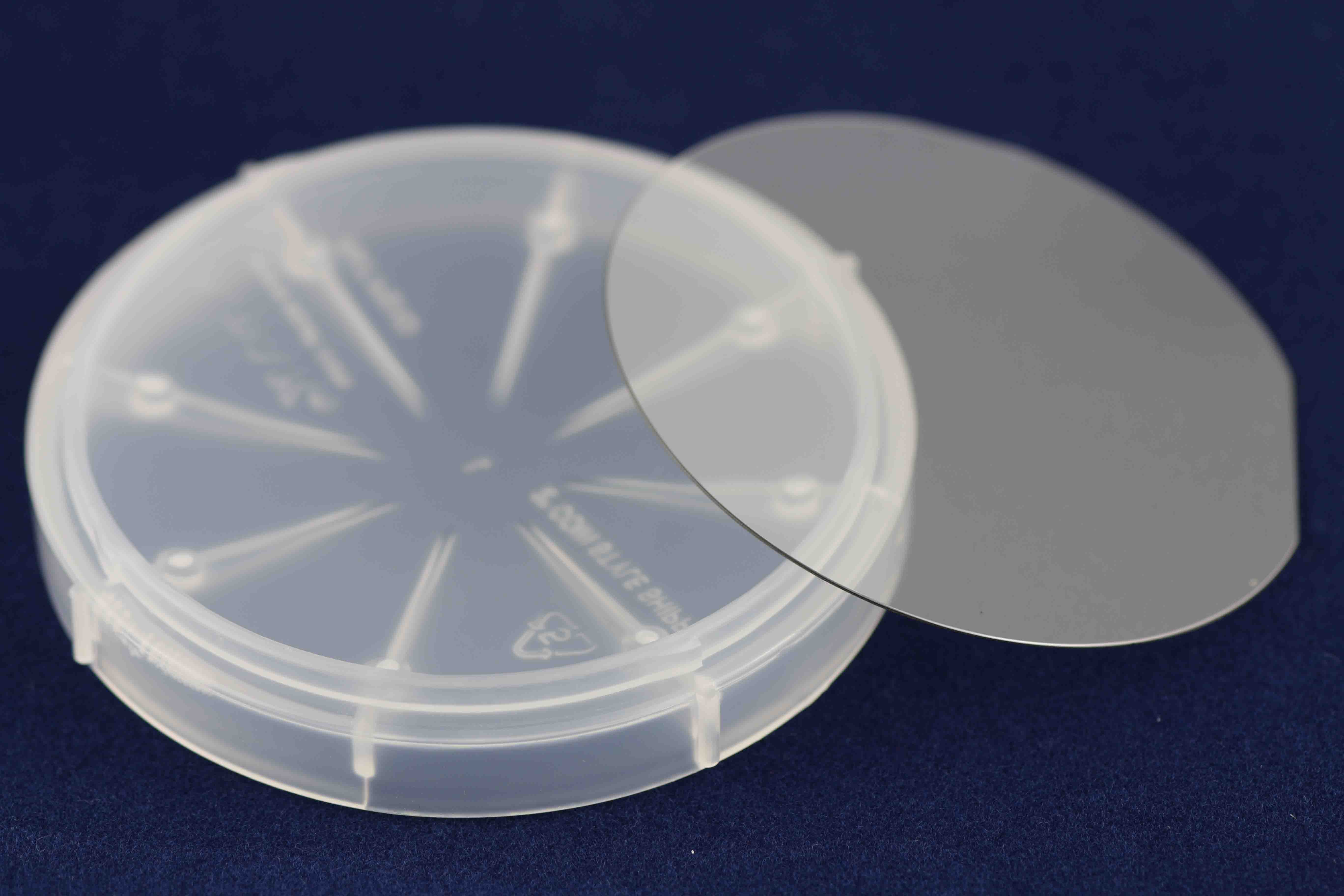
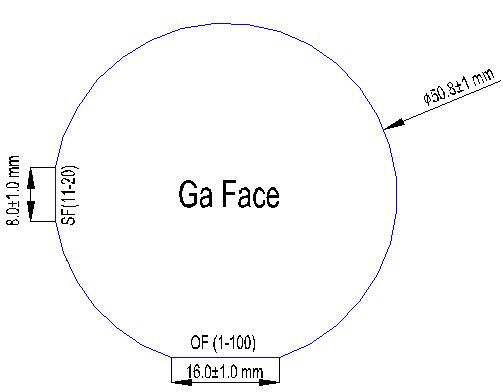
2 inch Free-Standing GaN Substrate
| Item | GaN-FS-C-U-C50 | GaN-FS-C-N-C50 | GaN-FS-C-SI-C50 |
| Dimensions | Ф 50.8 ± 1 mm | Ф 50.8 ± 1 mm | Ф 50.8 ± 1 mm |
| Thickness | 350 ± 25 µm | 350 ± 25 µm | 350 ± 25 µm |
| Useable Surface Area | >90% | >90% | >90% |
| Orientation | C-plane (0001) off angle toward M-Axis 0.35°± 0.15° | C-plane (0001) off angle toward M-Axis 0.35°± 0.15° | C-plane (0001) off angle toward M-Axis 0.35°± 0.15° |
| Primary Orientation Flat | (1-100)±0.5°,16.0±1.0mm | (1-100)±0.5°,16.0±1.0mm | (1-100)±0.5°,16.0±1.0mm |
| Secondary Orientation Flat | (11-20)±3°,8.0±1.0mm | (11-20)±3°,8.0±1.0mm | (11-20)±3°,8.0±1.0mm |
| TTV | ≤15µm | ≤15µm | ≤15µm |
| BOW | ≤20µm | ≤20µm | ≤20µm |
| Conduction Type | N-type | N-type | Semi-Insulating |
| Resistivity(300K) | < 0.1Ω·cm | < 0.05Ω·cm | > 106 Ω·cm |
| Dislocation Density | From 1x10⁵ to 3x106 cm-2 | From1x105 to3x106 cm-2 | From1x105 to 3x106 cm-2 |
| Polishing | Front surface:Ra<0.2 nm(polished); | Front surface:Ra<0.2 nm(polished); | Front surface:Ra<0.2 nm(polished); |
| or<0.3nm (polished and surface treatment for epitaxy) | or<0.3nm (polished and surface treatment for epitaxy) | or<0.3nm (polished and surface treatment for epitaxy) | |
| Back Surface:0.5~1.5μm; | Back Surface:0.5~1.5μm; | Back Surface:0.5~1.5μm; | |
| option:1-3nm (Fine ground); < 0.2nm(polished) | option:1-3nm (Fine ground); < 0.2nm(polished) | option:1-3nm (Fine ground); < 0.2nm(polished) | |
| Package | Packaged in a class 100 clean room environment, | Packaged in a class 100 clean room environment, | Packaged in a class 100 clean room environment, |
| in single container,under a nitrogen atmosphere. | in single container,under a nitrogen atmosphere. | in single container,under a nitrogen atmosphere. |
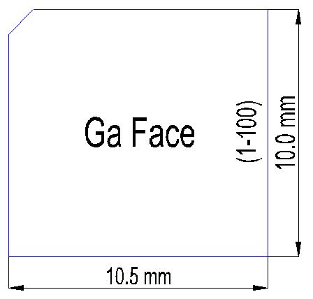
10x10.5mm2
Free-Standing GaN Substrate
| Item | GaN-FS-C-U-S10 | GaN-FS-C-N-S10 | GaN-FS-C-SI-S10 |
| Dimensions | 10×10.5mm2 | 10×10.5mm2 | 10×10.5mm2 |
| Thickness | 350±25μm | 350±25μm | 350±25μm |
| Orientation | C-plane(0001)off angle toward M-Axis 0.35°±0.15° | C-plane(0001)off angle toward M-Axis 0.35°±0.15° | C-plane(0001)off angle toward M-Axis 0.35°±0.15° |
| TTV | ≤10µm | ≤10µm | ≤10µm |
| BOW | ≤10µm | ≤10µm | ≤10µm |
| Conduction Type | N-type | N-type | Semi-Insulating |
|
Resistivity (300K) |
< 0.1Ω·cm | < 0.05Ω·cm | > 106Ω·cm |
| Dislocation Density | From 1x10⁵ to 3x106cm-2 | From 1x10⁵ to 3x106cm-2 | From 1x10⁵to 3x106cm-2 |
| Useable Surface Area | >90% | >90% | >90% |
| Polishing | Front Surface:Ra<0.2 nm(polished); | Front Surface:Ra<0.2 nm(polished); | Front Surface:Ra<0.2 nm(polished); |
| or <0.3nm(polished and surface treatment for epitaxy) | or <0.3nm(polished and surface treatment for epitaxy) | or <0.3nm(polished and surface treatment for epitaxy) | |
| Back Surface:0.5~1.5μm; | Back Surface:0.5~1.5μm; | Back Surface:0.5~1.5μm; | |
| option:1-3nm(Fine ground);<0.2nm(polished) | option:1-3nm(Fine ground);<0.2nm(polished) | option:1-3nm(Fine ground);<0.2nm(polished) | |
| Package | Packaged in a class 100 clean room environment, | Packaged in a class 100 clean room environment, | Packaged in a class 100 clean room environment, |
| in single container,under a nitrogen atmosphere. | in single container,under a nitrogen atmosphere. | in single container,under a nitrogen atmosphere. |
Non-Polar and Semi-Polar Free-Standing GaN Substrate
| Item | GaN-FS-A-U/N/SI-S | GaN-FS-M-U/N/SI-S | GaN-FS-SP-U/N/SI-S |
| Dimensions | (5.0~10.0)× 10.0 mm2 | (5.0~10.0)× 10.0 mm2 | (5.0~10.0)× 10.0 mm2 |
| (5.0~10.0)× 20.0mm2 | (5.0~10.0)× 20.0mm2 | (5.0~10.0)× 20.0mm2 | |
| Thickness | 350±25μm | 350±25μm | 350±25μm |
| Plane | (11-20) | (1-100) | (20-21) (20-2-1) (11-22) (10-11) |
| Miscut Angle | -1°±0.2° | -1°±0.2° | -1°±0.2° |
| TTV | ≤10µm | ≤10µm | ≤10µm |
| BOW | ≤10µm | ≤10µm | ≤10µm |
| Conduction Type | N-type < 0.1Ω·cm | N-type < 0.1Ω·cm | N-type < 0.1Ω·cm |
| N-type < 0.05Ω·cm | N-type < 0.05Ω·cm | N-type < 0.05Ω·cm | |
| Resistivity(300K) | Semi-Insulating > 106Ω·cm | Semi-Insulating > 106Ω·cm | Semi-Insulating > 106Ω·cm |
| Dislocation Density | From 1x10⁵ to 3x106cm-2 | From 1x10⁵ to 3x106 cm-2 | From 1x10⁵ to 3x106 cm-2 |
| Useable Surface Area | >90% | >90% | >90% |
| Polishing | Front Surface:Ra<0.2 nm(polished); | Front Surface:Ra<0.2 nm(polished) | Front Surface:Ra<0.2 nm(polished) |
| Back Surface:1-3nm(fine ground); | Back Surface:1-3nm(fine ground); | Back Surface:1-3nm(fine ground); | |
| option:<0.2nm(polished) | option:<0.2nm(polished). | option:<0.2nm(polished). | |
| Package | Packaged in a class 100 clean room environment, | Packaged in a class 100 clean room environment, | Packaged in a class 100 clean room environment, |
| in single container,under a nitrogen atmosphere. | in single container,under a nitrogen atmosphere. | in single container,under a nitrogen atmosphere. |
4 inch GaN Template
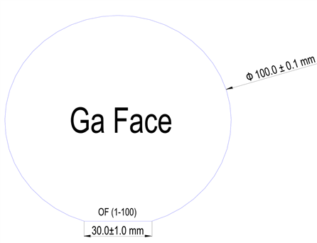
| Item | GaN-T-C-U-C100 | GaN-T-C-N-C100 |
| Dimensions | Ф 100 ± 0.1 mm | Ф 100 ± 0.1 mm |
| Thickness | 4.5±0.5 µm, 20±2 µm | 4.5±0.5 µm, 20±2 µm |
| Orientation | C-plane(0001) ± 0.5° | C-plane(0001) ± 0.5° |
| Conduction Type | N-type(Undoped) | N-type(Si-doped) |
| Resistivity(300K) | < 0.5Ω·cm | < 0.05Ω·cm |
| Carrier Concentration | < 5x1017cm-3 | > 1x1018cm-3 |
| Mobility | ~ 300cm2/V•s | ~ 200cm2/V•s |
| Dislocation Density | Less than 5x108 cm-2(estimated by FWHMs of XRD) | Less than 5x108 cm-2(estimated by FWHMs of XRD) |
| Substrate Structure | GaN on sapphire (standard :SSP option:DSP) | GaN on sapphire (standard :SSP option:DSP) |
| Useable Surface Area | >90% | >90% |
| Package | Packaged in a class 100 clean room environment, in cassette of 25pcs | Packaged in a class 100 clean room environment, in cassette of 25pcs |
| or single container , under a nitrogen atmosphere. | or single container , under a nitrogen atmosphere. |
2 inch AlN Template

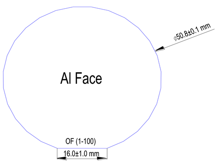
| Item | AlN-T-C-C50 |
| Dimensions | Ф 50.8 ± 0.1 mm |
| Thickness | 4±1.5µm |
| Orientation | C-plane (0001) |
| Conduction Type | Semi-Insulating |
| Crystalline Quality | XRD FWHM of (0002) < 350 arcsec |
| XRD FWHM of (1012) < 450 arcsec | |
| Surface Roughness | Ra < 5 nm (10 x 10 µm2) |
| Substrate Structure | AlN on sapphire (SSP) |
| Useable Surface Area | Exclusion zone< 2 mm |
| Package | Packaged in a class 100 clean room environment, in cassette of 25pcs |
| or single container , under a nitrogen atmosphere. |