Within these methods, multicrystalline materials are produced according to the “VGF” method. This is also known as “directional solidification”.
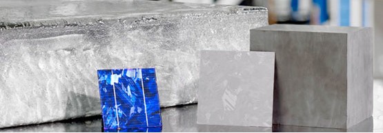
The polycrystalline pure silicon is melted down in a silica crucible via resistive heating. The slow cooling of the melt, where large areas of crystal with regular structure are formed, takes place in the melting crucible. The heated zone (temperature gradient) is slowly move upwards so that liquid silicon is present in the top area at the end of the process, whilst solidification into multicrystalline material takes place from the crucible bottom. Crystallization is controlled by the shifting of the temperature gradient. Until the temperature is cooling down, the brick is taken out and then saw into wafer.
Nowadays, the manufacturers of silicon based wafer put more emphasis on mono wafer due to the high efficiency rate. In fact, there are still a lot of advantages in the multi puller. One of them is that the multi ingot can be cut into full-square wafer directly which can ensure high capacity utilization rate. In addition, polycrystalline can produce approximately 450 to 600 kg or more than one ton ingot in one cycle time (about 50 to 60 hours) which shows that it has higher production rate. Due to these advantages, people still work hard to enhance the efficiency rate of multi wafer and make it more competitive.